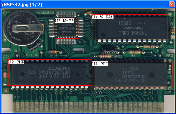
 |
What is this?On the PCB and chip pages, a window will appear along side for viewing the current PCB. On the PCB page, you can set the positions of each chip. This is already done for all PCBs in the system, but if you have a new one you can optionally set these. The purpose of these zones is for when on the chip page, upon selection of a slot, the image will zoom in on the chip, making it easier read, and less likely to be mis-identified. If you are in "Update" mode, the PCB scan attached to the web profile will be downloaded and displayed. If you are adding a new profile, it will attempt to find and load the correct PCB scan for you. If it finds more than 1 match, you can switch between them using the LEFT and RIGHT keys. Otherwise if no image is found, you can click in the window to open a file selection box. Upon profile submission, the scan selected in the window will also be automatically uploaded to the website, if you've enabled this feature in the settings. |
Window controls
| Right-click: | If the window is zoomed in, this will zoom out. Otherwise it will zoom in (to the original image resolution) centered on the point clicked, without performing any kind of selection. |
|---|---|
| Left-click: | This will attempt to auto-select the chip clicked on and will zoom in on the selection. This works kinda like a "flood-fill" operation in paint programs, using the outer-bounds of the fill as the selection rectangle. This usually works well, but if there are "obstructions" that it can't flow around, it may not select the whole chip. Conversely, if there isn't enough contrast between the color of the PCB and the chip, it will end up selecting too much. |
| + CTRL: | If the auto-select doesn't work right, CTRL-click 2 opposite corners of the chip. You must hold the CTRL key down between clicks. |
| + SHIFT: | Holding the SHIFT key while clicking will prevent the window from zooming in automatically. |
| BACKSPACE: | Will erase the rectangle for the current slot, or whatever rectangle was last created. |
| LEFT & RIGHT: | If multiple matching scans were found during the auto-search (indicated next to the filename), you can flip between them with these keys. |
| DOWN: | If zoomed in, this will flip the selection 180°. |
| ENTER: | Sets the coords of the current selection to the current slot. The saved coords do take into account if the selection was flipped or not. Additionally, if on the PCB page, the next slot will be selected so you don't have to go back and forth between windows. |
| F: | This will flip the entire source image. This is different than the DOWN key, this should only be used if your scan is flipped 180°, having the cart edge on top. This will allow the coords to match up with the image properly. If you're defining a new PCB, make sure the image is flipped to the correct orientation when settings coords (that is, cart-edge down). |
| Left-Doubleclick: | If you accidently open the wrong image (or the program does), you can double-click in the window to bring up the file dialog again. |
Text Orientation
When defining coords, be sure to make the text right-side up before pressing ENTER. Selections that are taller than they are wide (i.e. the chip is installed sideways), will automatically be rotated 90°.
You should set the coords of the PRG ROM first because depending on which side of the PCB it is on, that will decide whether or not to flip the image by default.
When selecting chips that are close to being square (like the MMC3), if the rect ends up being taller than wide, it will end up incorrectly rotating it. You can get around this by manaully selecting the rect and making sure that it is slightly wider than tall.
Coords are based on the window, not the image, and are relative to the center of the window. This way, as long as the source image is evenly clipped, the rects should scale pretty well into place regardless of the source image resolution.
| Return to Index |