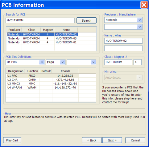
Step 2: Finding the PCB used
You will notice another window pops up on the screen while on this page. If you have the PCB scan auto-loader setup properly, your PCB scan for this cart will already be displayed (or one of them at least, if you have dupes of this cart). If there is no image displayed, click in the window to bring up a file selection dialog and select the scan yourself.
If the DB has any prior knowledge of the current game, a search will be run for likely candidate PCBs. If this game is new to the system, enter the PCB into the search field and run a search manually. Results will be ordered by what the DB thinks is the most likely results at the top.
* Pressing ENTER in the search field will perform the search, set the focus to the results, and select the first item. If the first result happens to be the right one, hitting ENTER again will goto the next page.
With any luck, it will find a match. In that case, just select the PCB from the list and move on to the next step.
If not, you will have to enter this data yourself. First off, if this new board is just a revision of another known board (e.g. you found a NES-SLROM-07 and the DB knows of NES-SLROM-06), make things easy on yourself and select the PCB your basing off from the list first. This will preload the fields on the page with data on this PCB. Then you can just make the necessary changes as needed.
 |
|
||||||||||||||||||||||||||
| Mirroring | |
If using a CopyNES, this will be auto-detected. If not, you have to define this yourself. If the PCB contains a couple small pads with the labels "H" and "V", one of them will be bridged with a blob of solder like figure #1 or with a trace like figure #2. Both example images have horizontal mirroring.
|
  |
PCB Slot Definitions
For each chip on the PCB, there must be a slot defined for it. The 4 components to the definition are as follows:
| Slot Designation: |
This is the description of the spot for the chip as it is printed on the PCB. It should consist of 2 parts, the chip "#" and a description of what the chip does. Sometimes the # or the description (or both) are not present or are hidden beneath the chip. In such cases you should try to make up some logical designations of your own, using the following conventions:
|
|---|---|
| Chip Function: |
The basic function the chip performs. This definition is used to map the chip to other fields.
|
| Default Part: | This is primarily used for MMC chips and is intended for emulator use so they don't have to differentiate between multiple part #'s when they all function the same. This especially applies to discrete logic parts as they are made by a large number of manufacturers, all with different part #'s. The value here will be mapped into the "Hardware" field in the hardware details section. If it is left blank, the actual part # will be used. Default values for epoxy parts should be enclosed in < > brackets. ROM's and RAM's do not use this field. |
| Chip Co-ordinates: | These are set via the scan preview window and is discussed further on the PCB Scan Window page |
Slot Manipulation
The 3 combo-boxes above the slot list from left to right are: Designation, Function, and Default. When the designation changes, it will look for appropriate values to enter into the other 2 fields. You should enter these in the same order as the # in the designation.
* Pressing the ENTER key in any of these 3 fields will add the values to the slot list below and reset the focus to the designation combobox.
To remove a slot from the list, select it and press the DELETE key.
To rearrange the list ordering, select the slot you want to move and use the PAGE UP and PAGE DOWN keys to move it up or down, respectively.
Before setting any chip coords, you should define all the slots first.
| « Previous Page | Return to Index | Next Page » |